All the measurements in this document are based on the following schematic diagram with the values and part numbers stated on it. The circuit was tested with Samsung Galaxy S7 cellular phone.
The DATA connector of Yaesu FT-817 has two data output pins: pin 3 for data rate of 9600 bps with maximum output level of 500 mVpp and pin 4 for data rate of 1200 bps with maximum output level of 300 mVpp. The latter is used in most HF communications.
The output from the transceiver is fed to the circuit through R13 to the R10 trimmer potentiometer which adjusts the input signal level. Then through R8-C2-C1 network it is fed into the base of Q1 (amplifier stage). Collector current of Q1 follows voltage changes on its base and causes voltage changes on the microphone pin of the phone. In this mode the circuit emulates an external microphone.
The amplitude of these changes is about 10-20mV which is enough for the software to decode it. At the same time this amplitude is too low to open D1 and D2. As a result, no DC bias appears on the base of Q2 and the PTT line of the transceiver is not pulled down.
Pin 4 of the DATA connector is used for feeding the data into the transceiver. According to the user manual of Yaesu FT-817, data rate of 1200bps requires input voltage of only 40 mVpp. Headphones output of a phone or tablet is usually capable to provide more than 1 Vpp which is more than enough.
In transmitting mode, the headphone output voltage from the phone passes through R1/R2-C2-R9 network to R11 which adjusts the transmitted signal amplitude. From the wiper of R11 the transmitted signal reaches the transceiver input through R14.
The signal from the phone's output also reaches Q1 base through R1/R2-C1. It is amplified by Q1, rectified into a DC voltage by voltage doubler C4, D1, D2 and filtered by C6. The voltage on C6 causes current flow through R12 and the base of Q2. R12 is a current-limiting resistor.
Collector current of Q2 keys the transceiver by pulling down the PTT line. The schematics of FT-817ND show that its PTT line is connected to 5V through a resistors network with the total resistance of 11kOhm. Thus the collector current of Q2 should be
5 V / 11 kOhm = 0.45 mA
The datasheet of 2N2222 states that DC current gain hFE will be 35 in the worst case. It yields the minimum base current of
0.45 mA / 35 = 0.012 mA = 12 uA
As will be shown later, this current is much higher.
Samsung Galaxy S7 provides 2.8VDC on the microphone input when it is open-circuited and 1.2mA short-circuited. Thus 1.2mA is the maximum current that the discussed circut will be able to draw from the phone.
With the circuit is connected to the phone, the voltage drops to 2.0V. The collector voltage of Q1 is 0.86V and the total current drawn by the circuit is
(2.0 V - 0.86 V) / 3.3 kOhm = 0.35 mA
When the collector resistor R6 is replaced with 2.2kOhm, the voltage on the microphone pin decreases to 1.87V and the collector voltage increases to 0.93V. The collector current becomes
(1.87 V - 0.93 V) / 2.2 kOhm = 0.43 mA
Reducing the value of R6 results in higher DC voltage on C6 when the same input signal amplitude is applied to the input. One possible explanation to this behavior is that a higher current through R6 is able to charge C6 to a higher voltage.
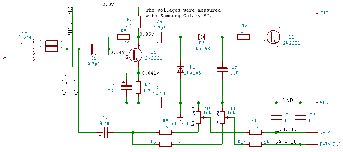
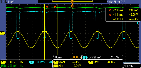
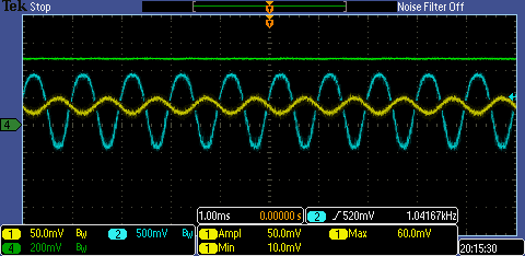
This section shows waveforms at different frequencies generated by DroidRTTY. The frequencies stated are mark frequencies. Space frequencies are 170Hz higher. Otherwise stated, the volume on the phone was set to maximum.
Trace colors on the oscillograms represent the following signals:
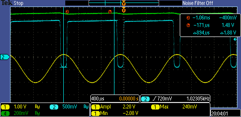
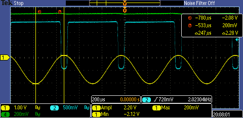
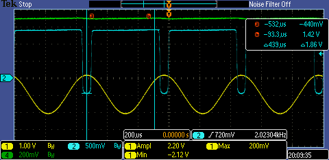
- yellow: amplifier input at the base of Q1
- cyan: amplifier output at the collector of Q1
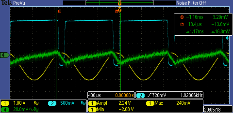
- green: rectified DC voltage on C6
The reference point is on the transceiver ground i.e. minus of C5 and emitter of Q2.
Some points to note:
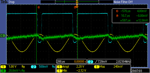
- Input voltage amplitude is 2.28Vpp. If we connected 32 Ohm headphones we would obtain 20mW of audio power.
- Output vaveform shows that when transmitting, Q1 functions as a switch rather than as a linear amplifier. In transmitting mode this isn't important because the output voltage is rectified.
- The rectified DC on C6 isn't smooth and shows ripple of about 72mV. It shouldn't affect the PTT switching stability but still is an interesting point to note.
- DC is 648mV at lowest point. Taking base-emitter voltage of Q2 as 0.6V and R12 as 1kOhm, base current is
(0.648 V - 0.6 V) / 1 kOhm = 0.048 mA = 48 uA
resulting in collector current of 0.048 mA * 35 = 1.68 mA which is at least three times more than required to key the FT-817.
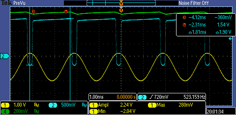
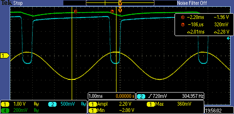
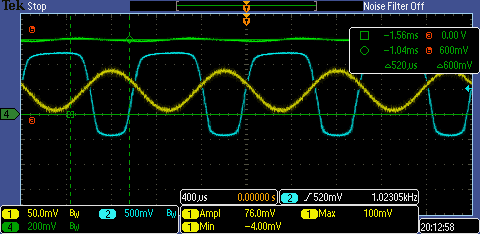
Here we see that the ripple voltage on C6 is smaller than on 250 Hz and is 32mV. Other parameters didn't change.
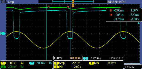
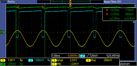
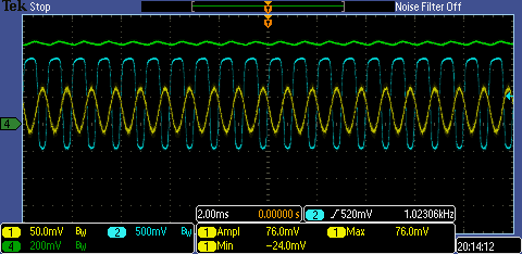
The ripple voltage on C6 became 16.8mV.
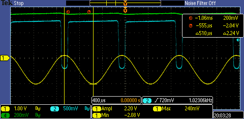
The ripple voltage on C6 became 12.8mV.
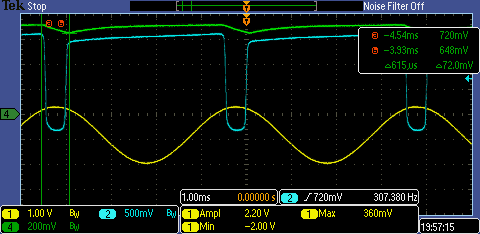
The next test was done with output frequency of 1000 Hz and output volume set to about 50%.
The input amplitude is about 75mVpp. The output amplitude almost did not change but the duty cycle became closer to 50%.
Rectified DC voltage on C6 is 600mV with the ripple of about 30mV.
The next waveforms were taken with output volume set to about one third.
They show relatively clean sinusoidal signal on the output. The rectified DC is 488mV which is not enough to drive Q2 into saturation.